Do not hesitate to contact me via e-mail ([email protected]) if you have any question or comment. If you see an error, you can issue a pullme request om my github
My smart switch project
The smart switch project
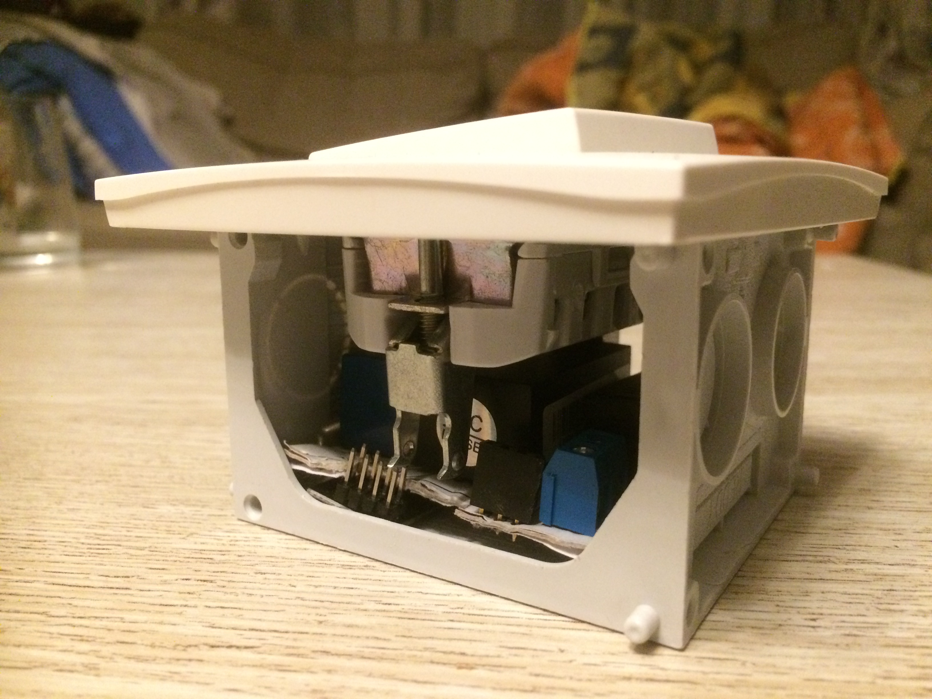
As an electronic enthusiast, I wanted to make a project which would involve creating my own PCB. Making a smart switch was the best project I could find.
The smart switch I had in mind has the following requirements:
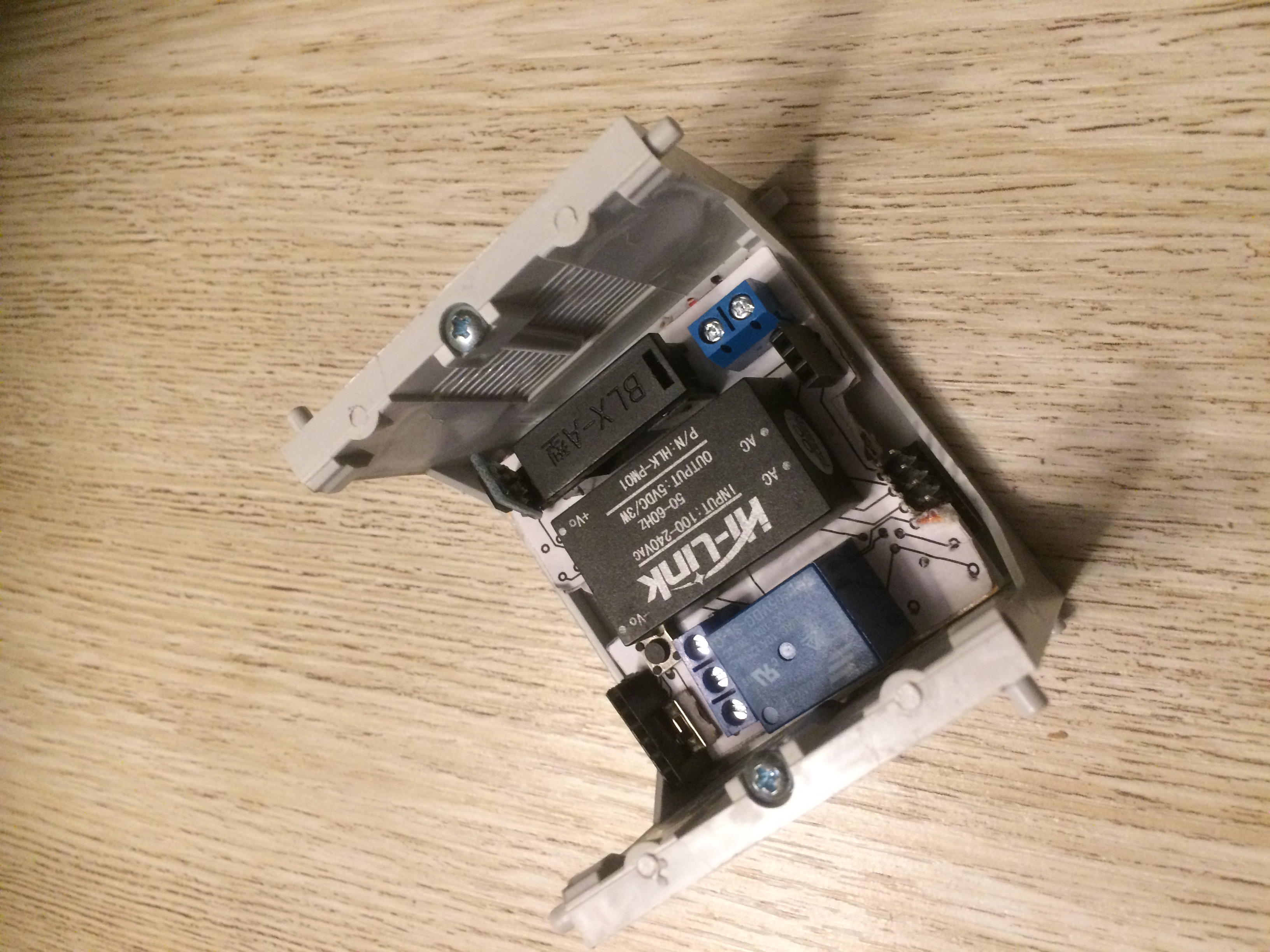
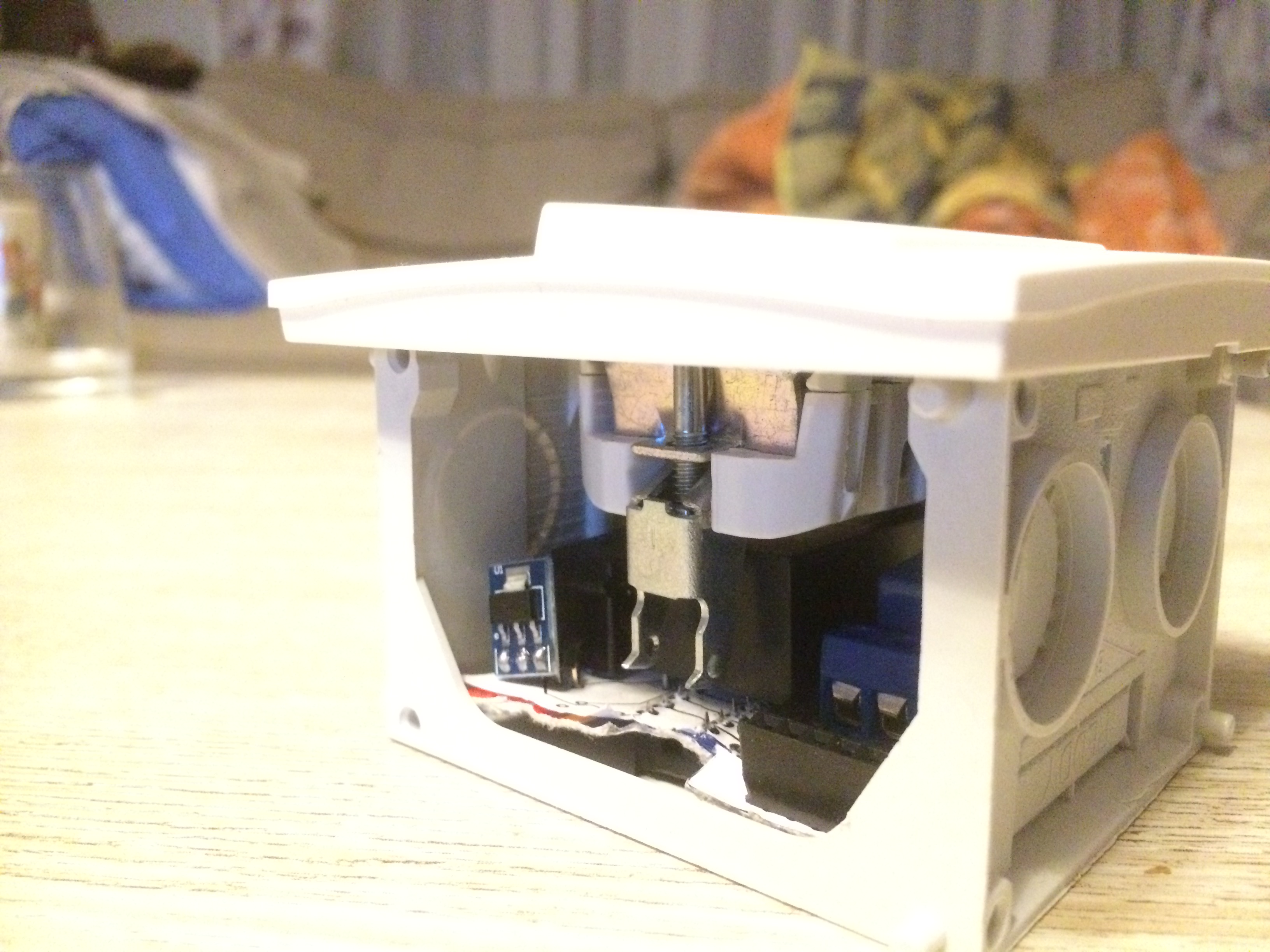
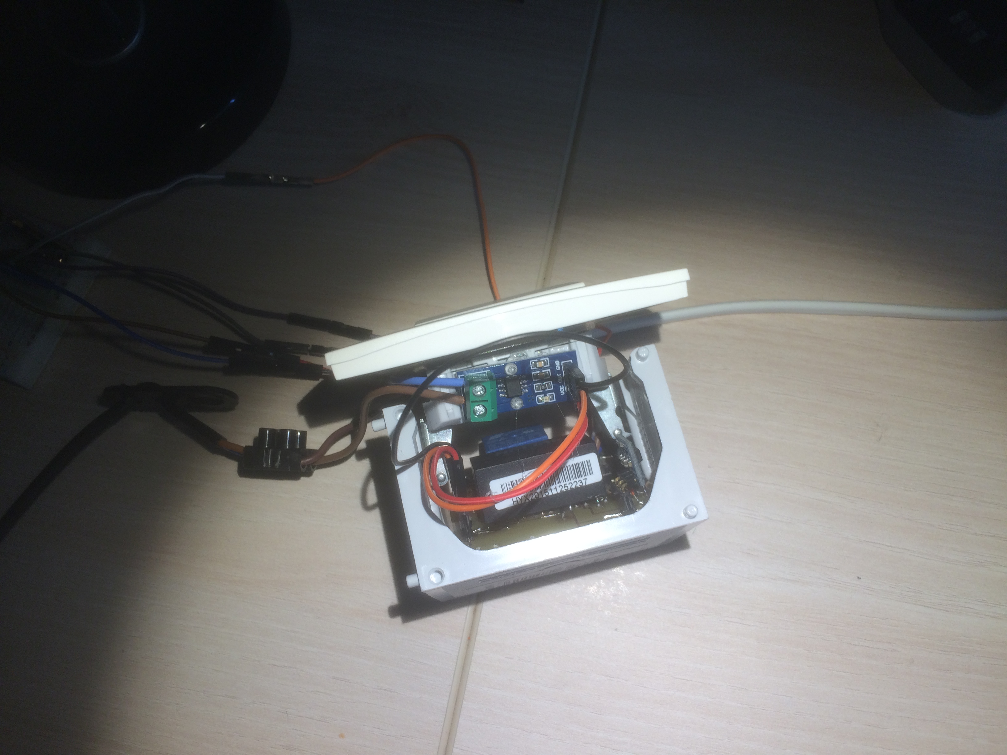
- Must fit into a wall switch case box
- Must be as less invasive as possible. Which means I did not want to change anything in my electrical installation, e.g to change my regular switches to push button switches.
- The physical switch must be available and functional (you don’t want your wife to be angry with you because she can’t open a light without her cellphone ;) )
- Even if my smart switch is blocked or dead, the physical switch must still work
The simplest idea that I got is to implement a 3 way switch configuration but embedded inside my switch box. That is, the physical switch would control one side of the 3 way switch and a micro-controller with a relay switch would control the other side. Surprisingly enough, I didn’t find any project that would implement such configuration. Was my idea too simple or too dummy? Had I overlooked something? I decided to try myself and discover it.
List of material
To make this project, my plan is to use the following component:
- Atmega328-28p (I did not use an arduino nano or mini, see below why)
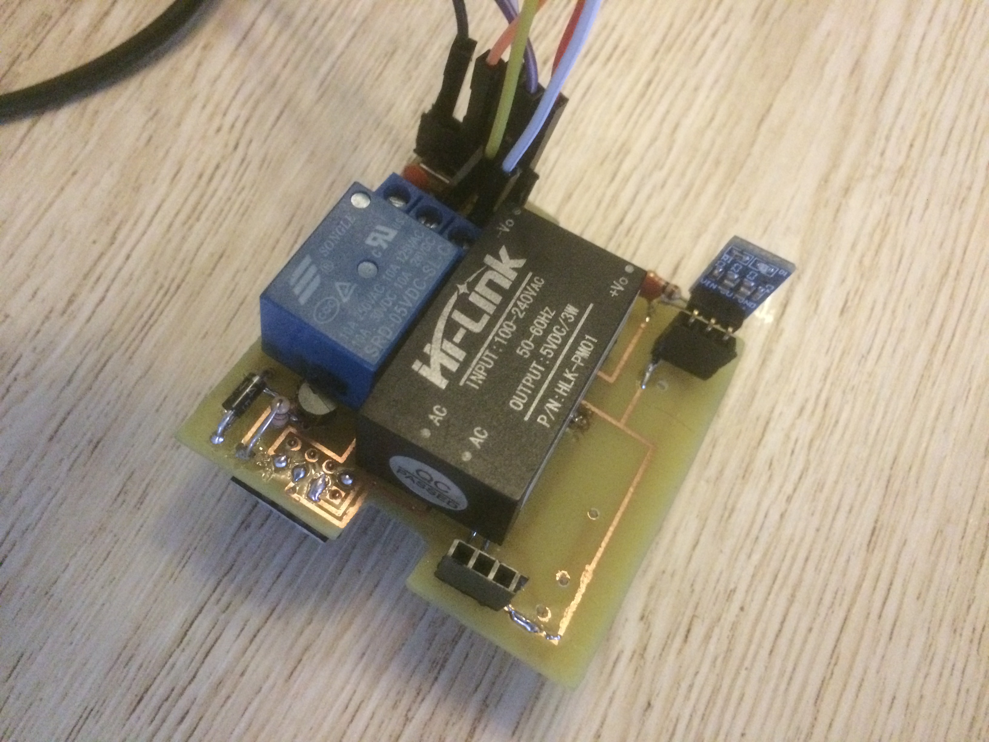
- SRD-05VDC-SL-C Relay
- A 2N3904 transistor to control the relay
- NRF24L01 for RF transmission
- HLKP01 as power supply
- ACS712 module to measure the current. Current is measured thanks to the Hall effect.
- Usual component such as voltage regulator, resistors, capacitors
Initial PCB layout
I quickly realized that due to space size, I will not be able to fit a full Arduino nano or mini into my switch box. Same conclusion for the SRD-05VDC-SL-C relay which usually is shipped on a breakout board.
As such, my project already challenged me as I didn’t know how to use the Atmega328-28p without its Arduino PCB. Same for the SRD-05VDC-SL-C relay without its breakout board.
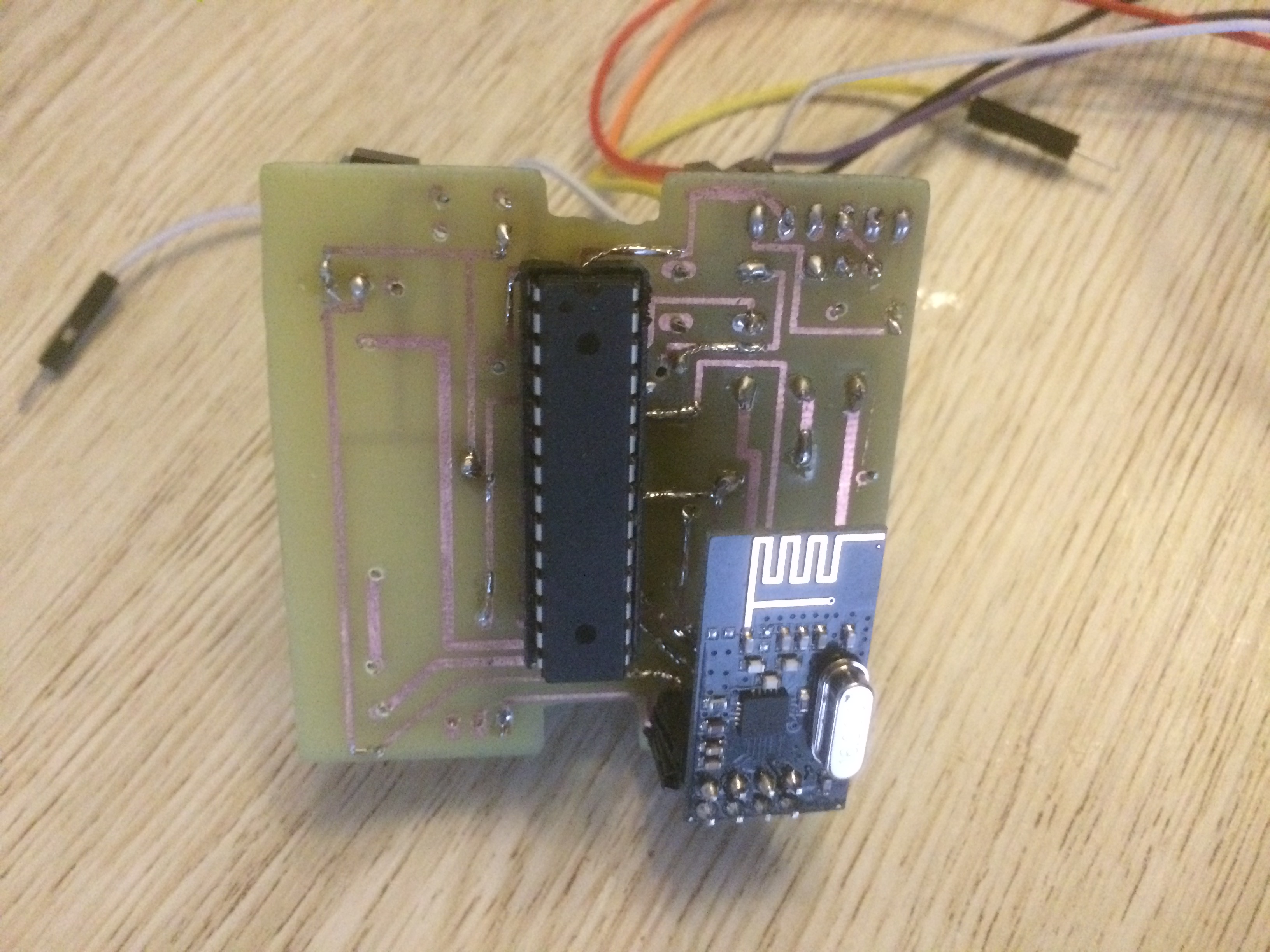
For the Atmega328-38p, I learned that it has an embedded 8Mhz clock. But in order to use it, we need to burn a specific bootloader. All the info on how to do that is explained on the arduino website. (see the last section about eliminating the external clock). It worked like a charm for me.
Then I had to understand how to wire up the standalone Atmega328-28p. To do so I checked how it was done on the Arduino board. What I did is to wire the following part of the Arduino mini datasheet
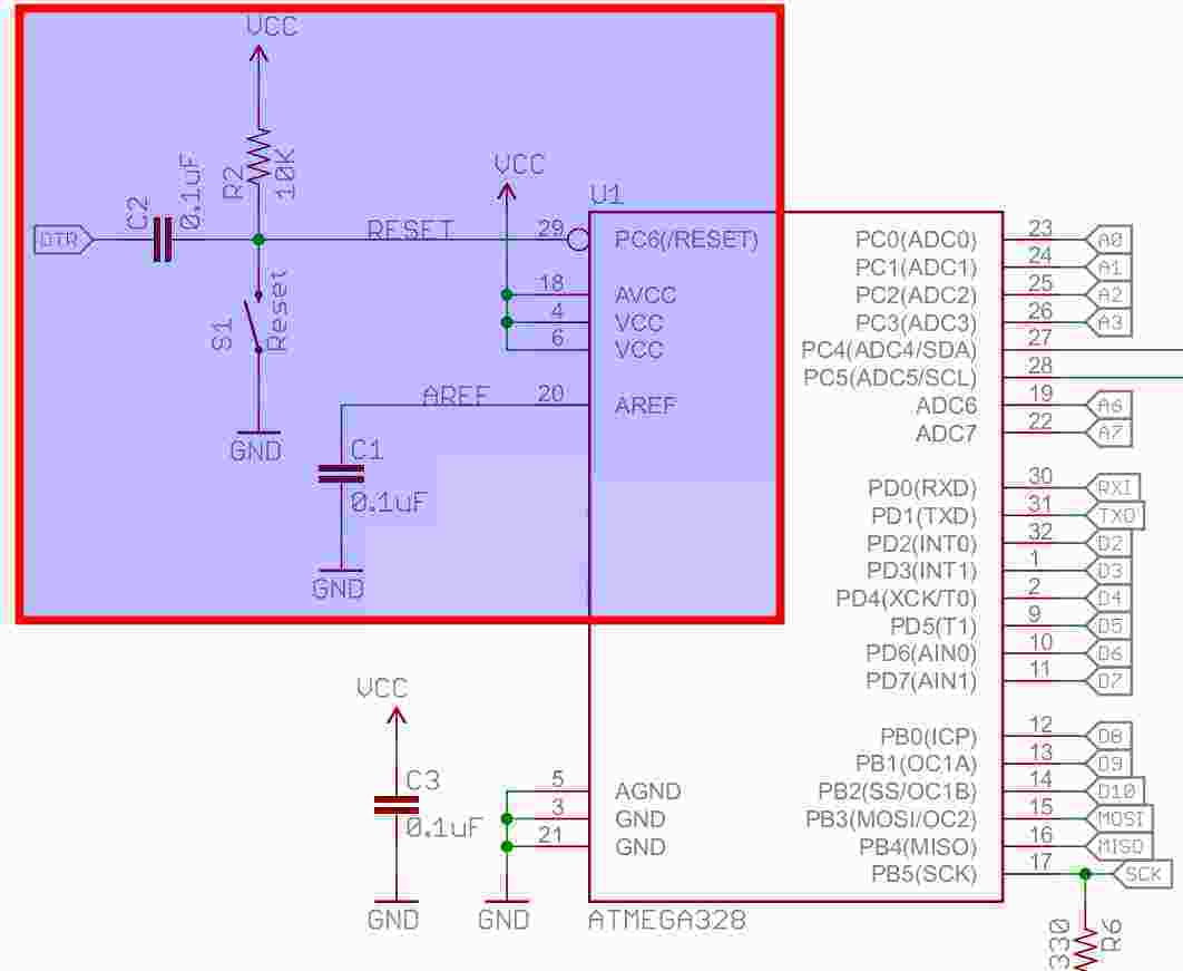
After that, I could program the Atmega328 using the FDT232RL breakout board and the Arduino uploader. The correct connection from the FDT232RL to the Atmega328-28p’s pins are:
- DTR -> DTR
- GND -> GND
- VCC -> VCC
- RX -> Tx
- TX -> RX
For the SRD-05VDC-SL, I found via a forum a link to a page where they are explaining how to wire the SRD-05VDC-SL (Thanks web archive).
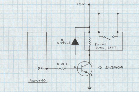
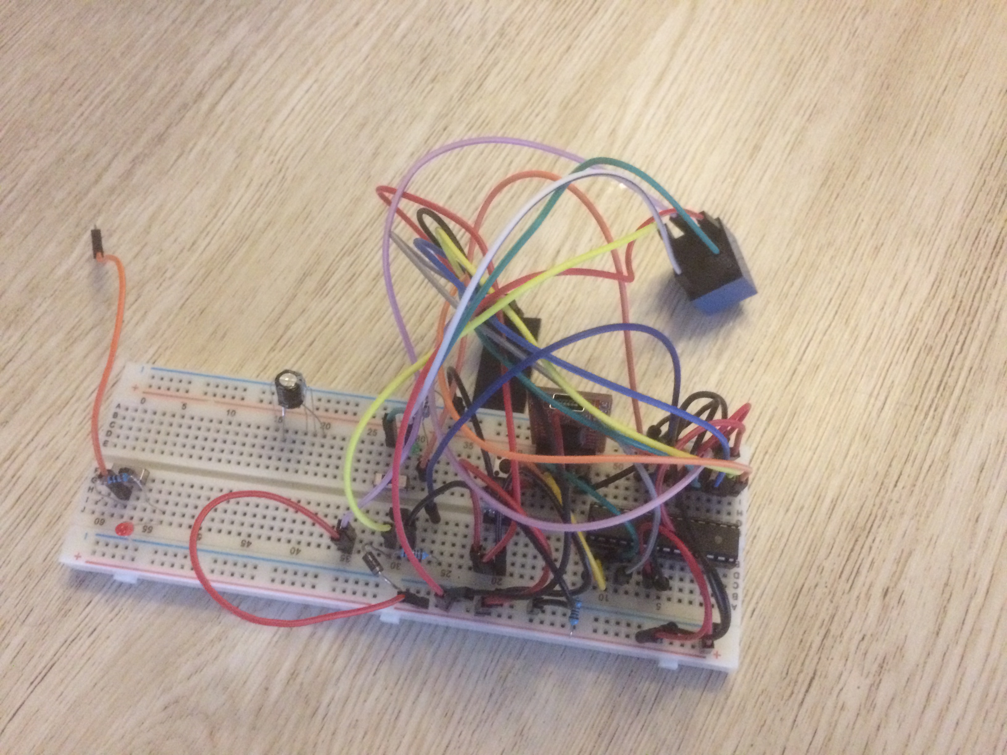
Time to test my design and my breadboard looked like this:
Quite messy isn’t it? But this first proof of concept turned to be a success.
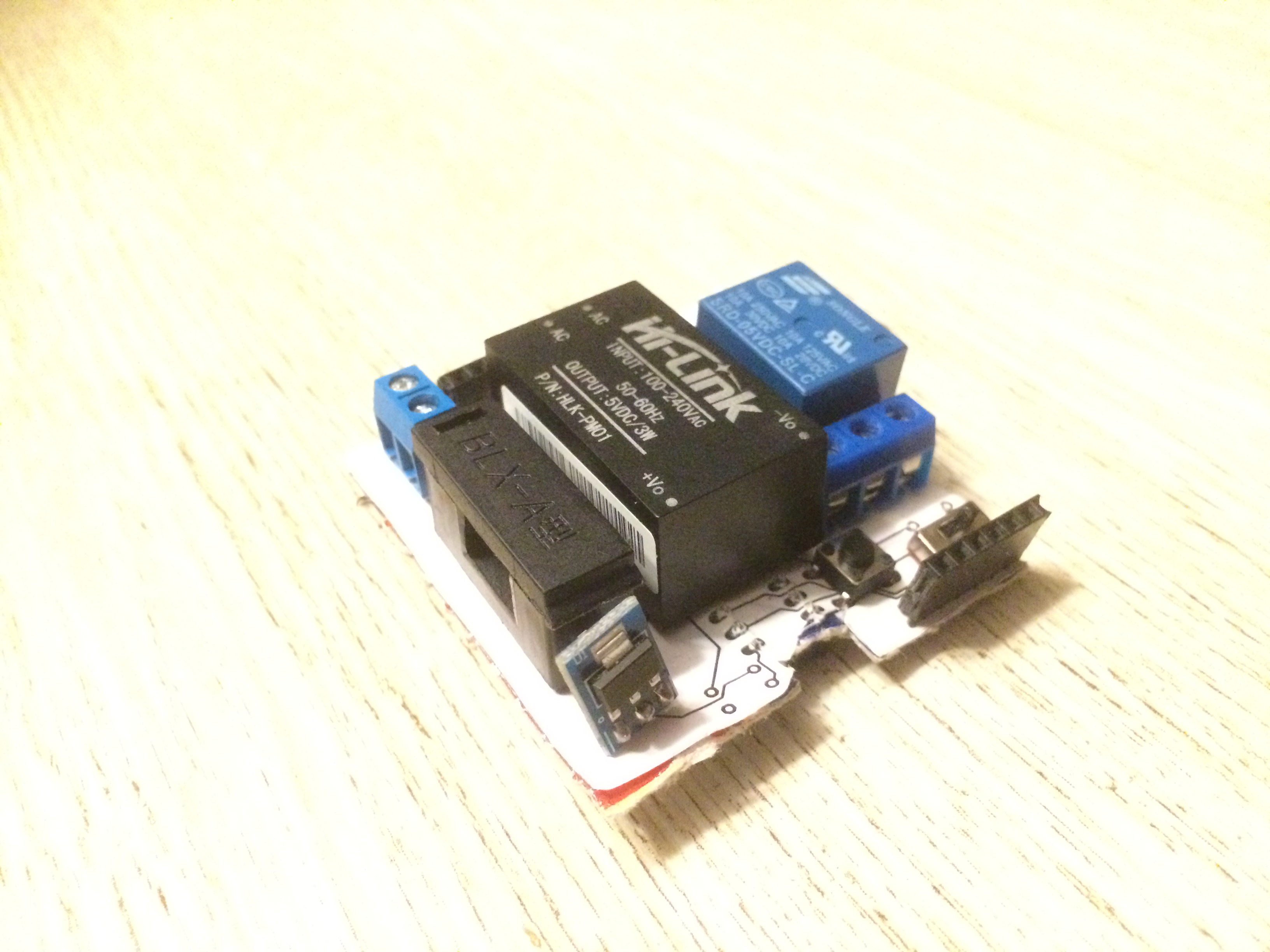
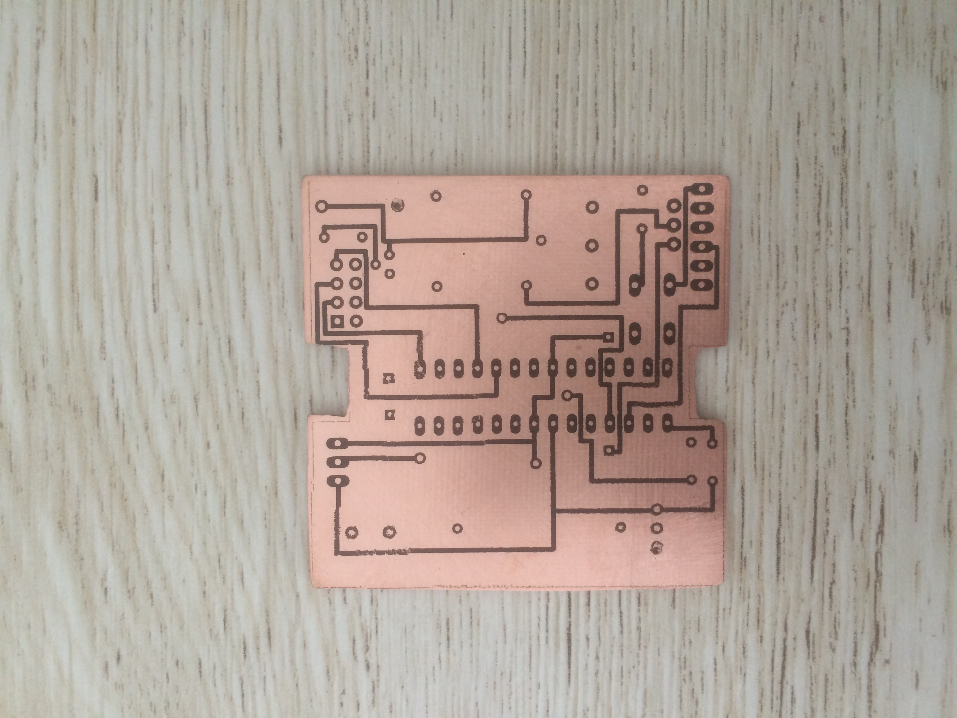
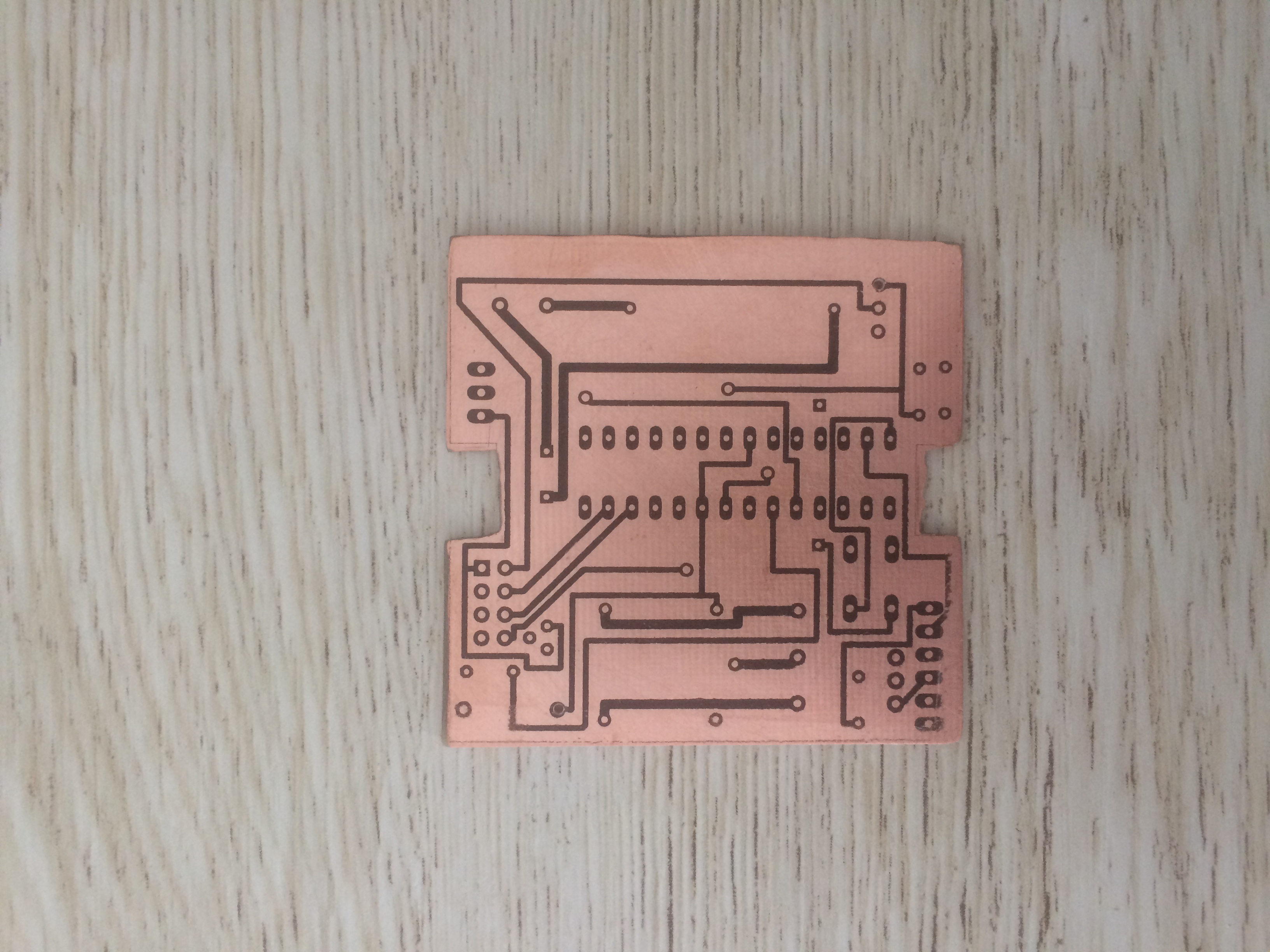
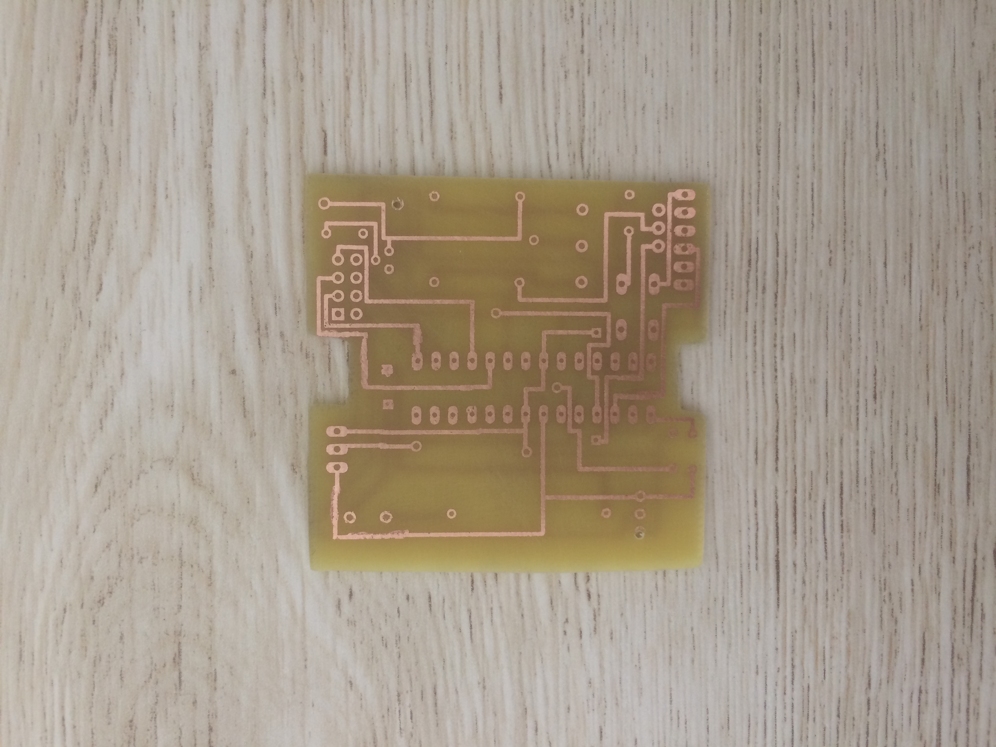
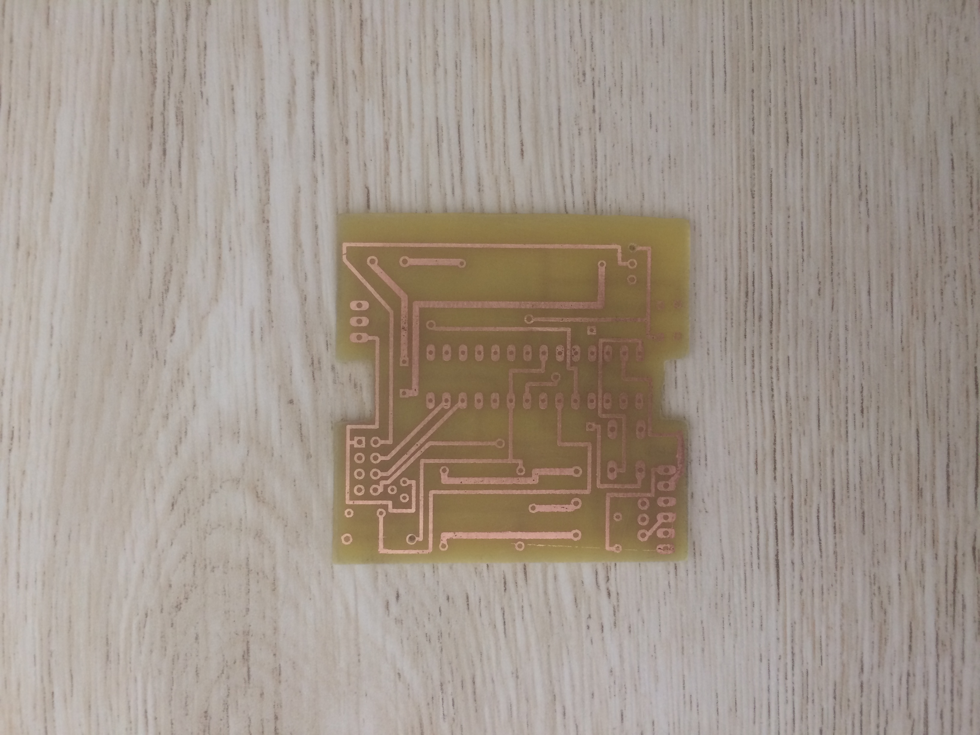
Eventually, I was ready to make my initial PCB. I began to make a PCB layout in Eagle and then to test how the components would fit in my switch on a simple carton sheet.
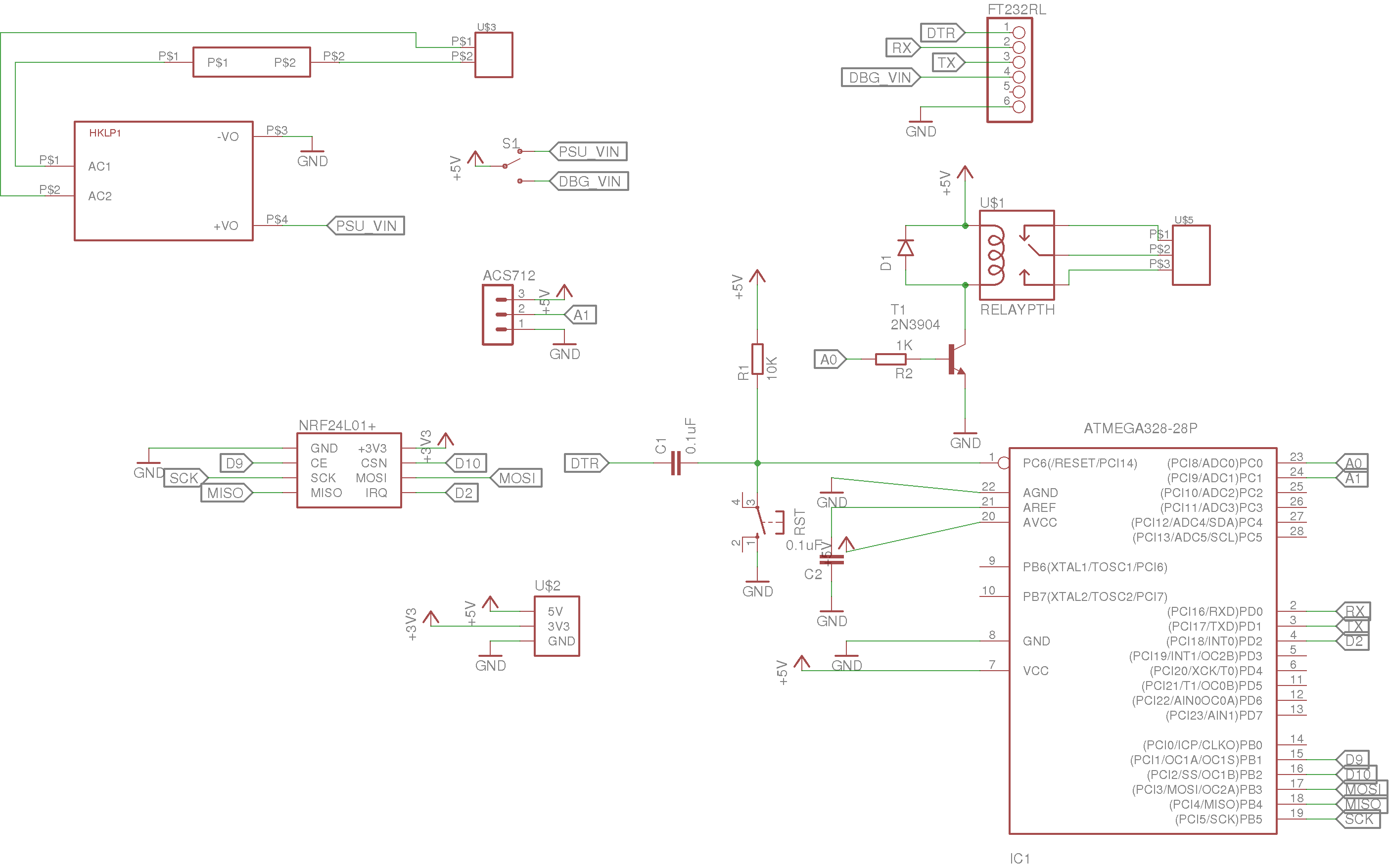
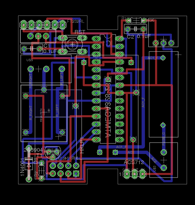
On the Eagle design, I had to wire everything by myself because I needed to have big routes (due to the PCB printing method explained bellow) and the Eagle autorouting functionality didn’t find any solution to connect everything.
First part of the design was completed. It was time to begin the second step which was to print my PCB
Print that PCB!
First of all, why did I want to print my PCB while we can order it for few boxes on the internet? Main reason was: DIY! I wanted to get that kind of experience. Second reason was, what if I made a mistake? Ordering 1 PCB sample is not possible or too expensive. You must order them by 5 or 10. If I screw something, then I’m having a bunch of useless PCBs.
I read about several methods to print homemade PCBs and I decided to go with the technic where the PCB layout is printed with a laser printer on a transfer paper, then the printed PCB is transfered to a piece of copper board with an iron and eventually, the copper is itched with a ferric chloride solution. Because of the knowledge buildup, I had to redo each of the steps at least 2-3 times to find the way that works for me.
PCB transfert
I learned during this step that the choice of paper is crucial! On the internet, we can read that people use photo paper, or glossy newspaper but both of the supports failed for me. I discovered we can buy from China a specific paper for PCB transfer purpose. Here is a link on Aliexpress that illustrate the kind of paper I’m talking about. It is super cheap and damn efficient! It just worked out the first time. In order to avoid the yellow paper to stick to my iron, I placed a sheet of kitchen paper in between the paper and the iron.
PCB etching
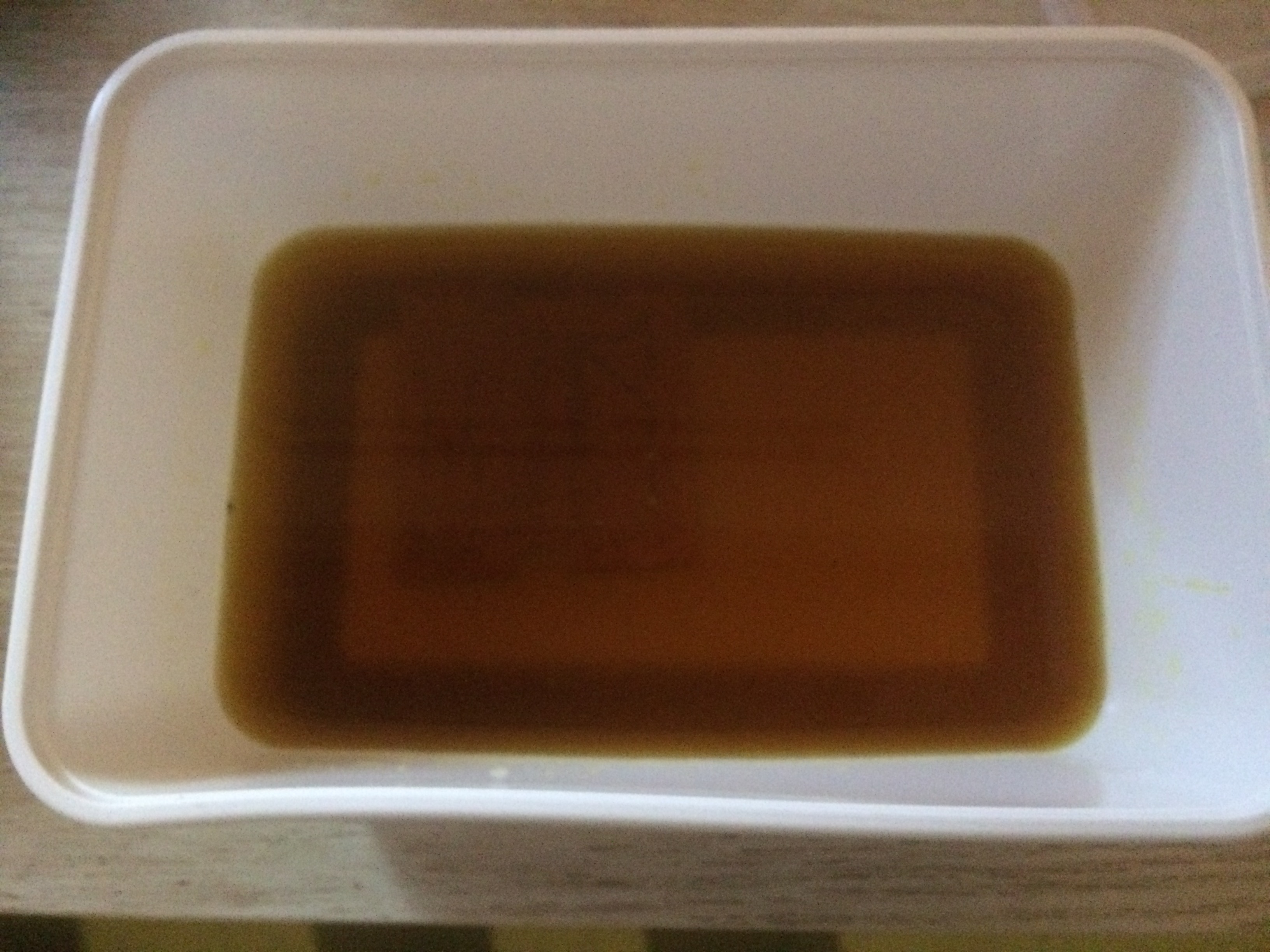
The next step consists of itching the PCB. For that purpose, I used a ferric chloride solution (FeCl3). The important thing in this step is to “wave” the solution over the PCB inside the bucket in order to etch the copper. If you don’t do that, it will take ages and eventually too much copper will be etched and your PCB will not work because routes between components will be broken.
During that step, make sure you are working in a ventilated environment with proper hands and eye protection.
If you wonder how I printed a double side PCB, I first transfered the top of my PCB, then I drilled two holes and I pierced the same holes on the yellow paper transfer. After that, I maintained the bottom part and the transfer paper in place by inserting a small long object and began the transfer with my iron. I finished up by removing the holding objects and completed the transfer using the same method as the first side.
Soldering the PCB
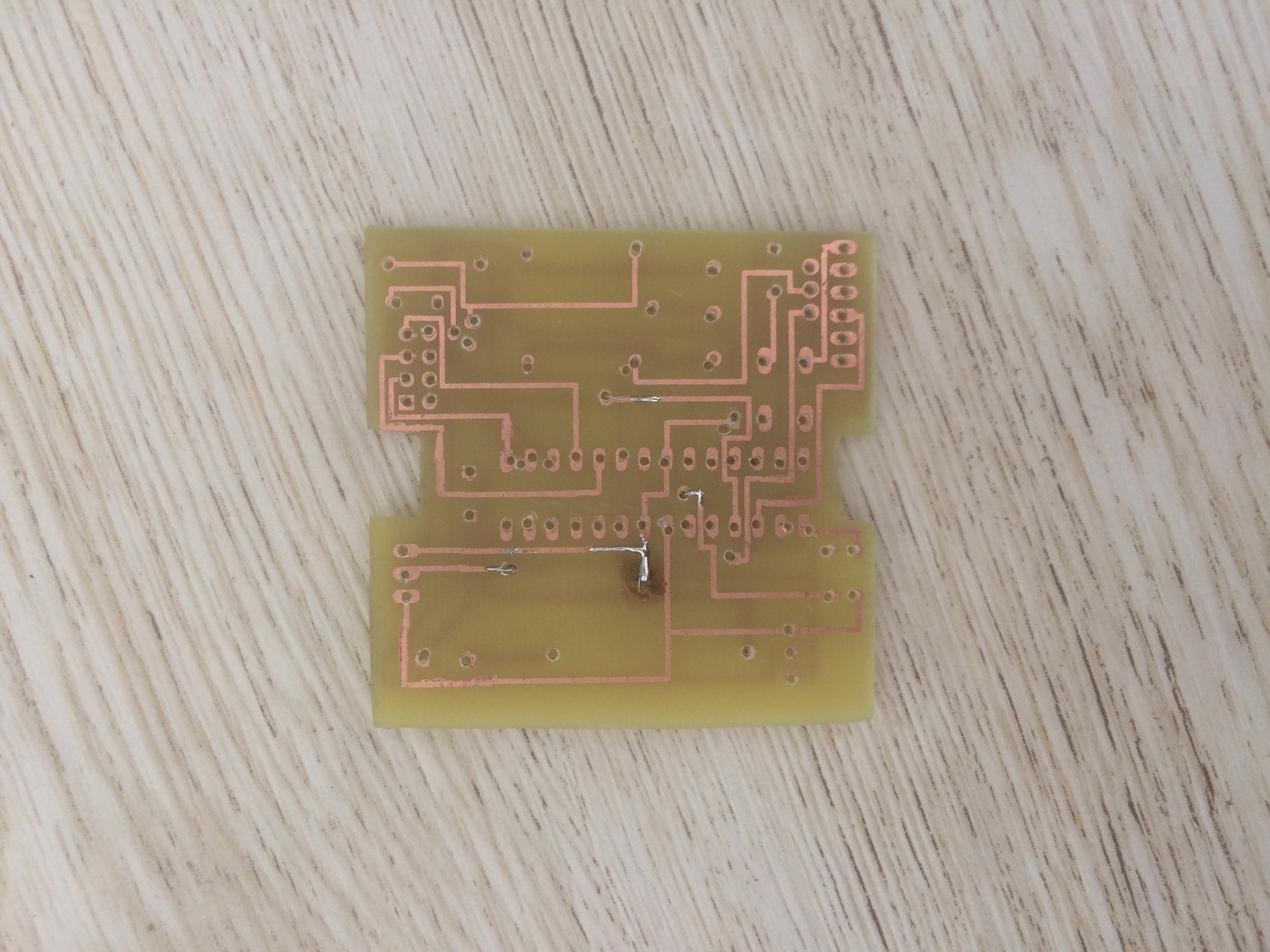
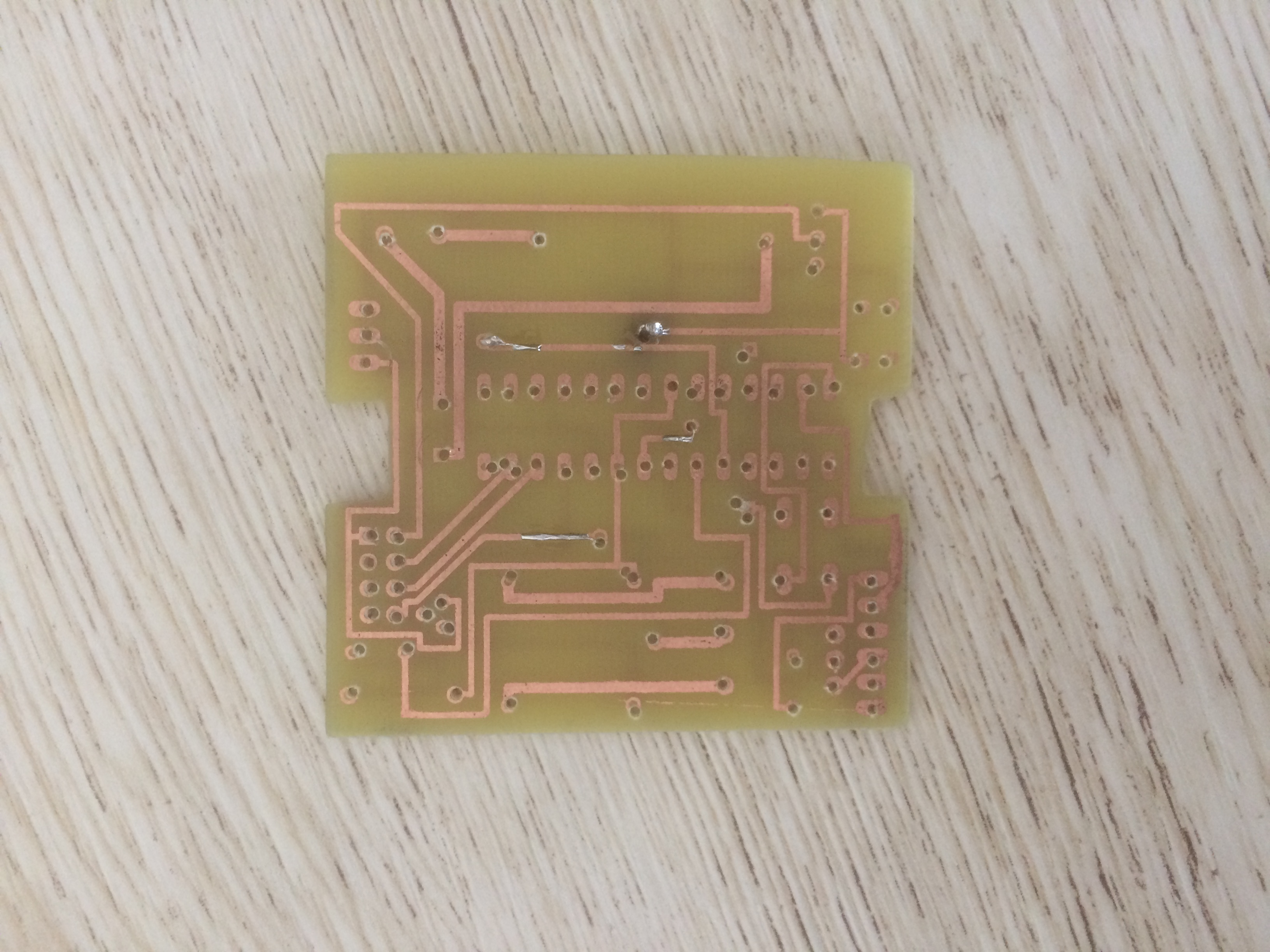
Next challenge was to solder the PCB. Making a PCB yourself has the disadvantage that both side of vias or pcb holes are not interconnected.
In order to solder the vias, I used small wires that I passed into the vias and that I soldered on each side of the pcb. By this means, I was able to get good connection through my vias.
To solder the components and make sure both sides where connected, I followed the same principle. I first solder a small wire on the component’s pins before soldering the component on the PCB. After that, I wired the small wired to their respective PCB routes.
Show time
First of all, the software I’m using to run my node is using the MySensor library. If you don’t know it yet, go on their website and have a look. They really have interesting projects.
Time now for testing. At first glance, I realized that I didn’t switched the RX and TX line in between the FDT232RL and my Atmega328 at the PCB level. As a consequence, I couldn’t see any output. Hopefuly enough, it is an easy fixable mistake by using regular jumper cable. The second issue I got was that the communication in between my node and my gateway was not working properly. It happens that the connection is much more stable if you mount a decoupling capacitor in between VCC and GND on the NRF24L01 input.
Those problems being solved, I decided first to retest lightning up a LED. As the following video demonstrate, the result is very good. Have a look at the feedback on the cellphone when the manual switch on the breadboard is activated.
However, when trying with a 220V light bulb, something is going wrong.
The first issue which is obvious is that there is a huge delay in between the time I pressed the button on the cellphone and the time the light switch on. My first guess is that there is some noise coming from the lamp high voltage and the RF has to issue packet retransmission. In the video, at one moment in time, the light switch off with no reason, most likely due to faulty communication in between the node and the gateway.
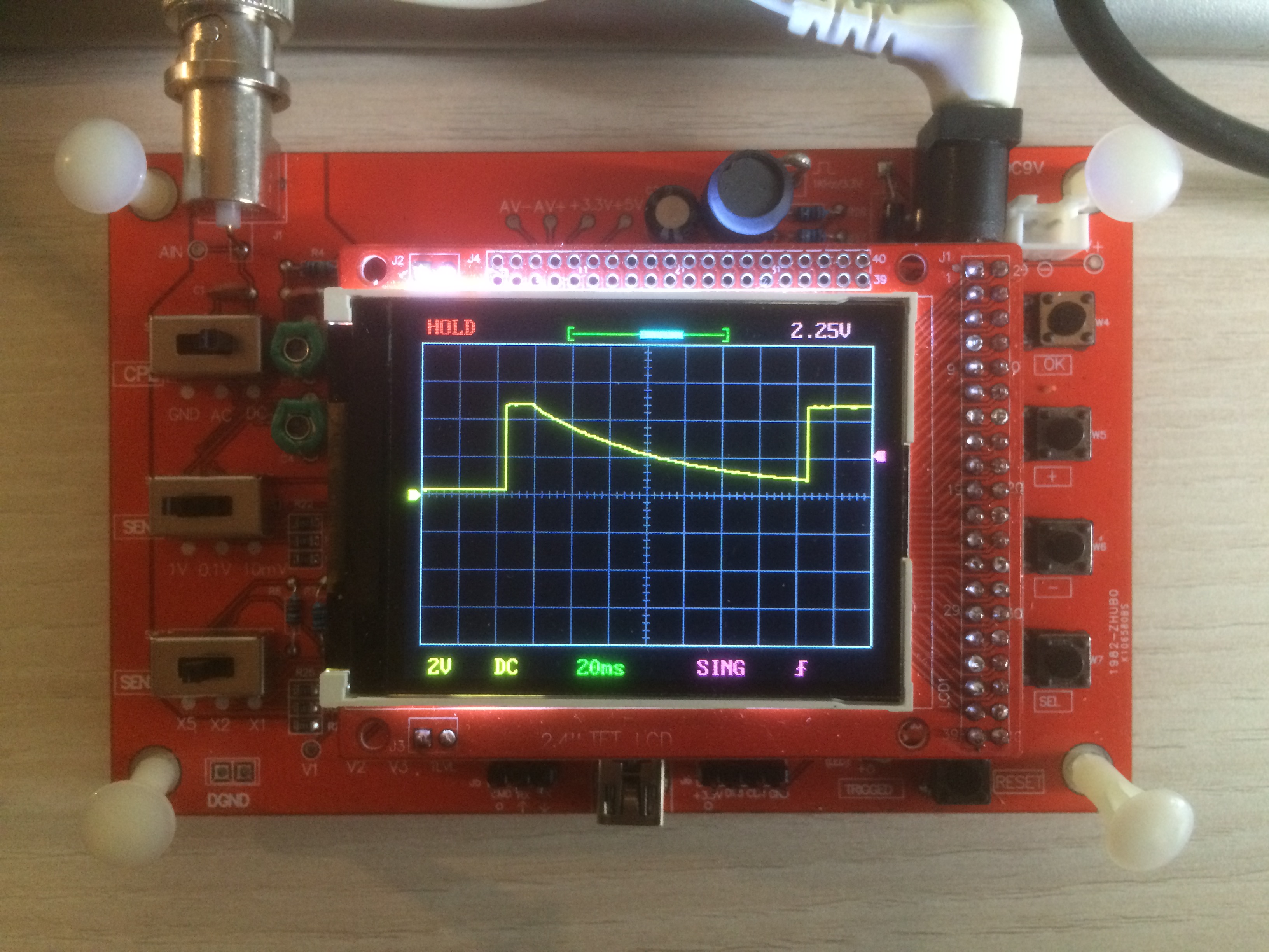
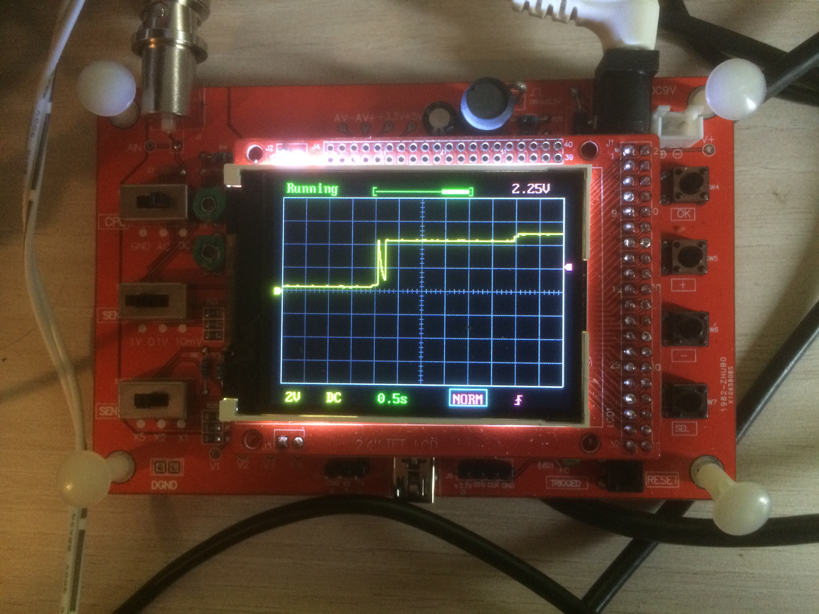
The second issue that I have is that the serial connection is not stable. Whenever the light switch off, the serial connection is dropping. By connecting an oscilloscope, I noticed that there is the DTR signal of the FDT232RL which is going high for no reason. Again here I believe the high voltage of my lamp is generating noises and this is reflected as having a voltage on that pin.
Note that the fact that I’m seeing this wierd behavior of my DTR signal is maybe a consequence of other things going wrong. Story to be continued…
Conclusion
It was an amazing journey! I learned a lot of things. Yet I do not have a 100% working solution, but the results that I have are very promising.
Full source code and full design is available on the github repository I made for that purpose.
